Report on Masterseminar EVA Semiconductors ‘23

28.11.2023

Fabrication and Test of Semiconductors

The Seminar on Test and Fabrication of Semiconductors is part of the Master of Science in Engineering MSE in Electrical Engineering. The aim is to provide interested students insights into the design, fabrication, and testing of semiconductor devices.

OLYMPUS DIGITAL CAMERA

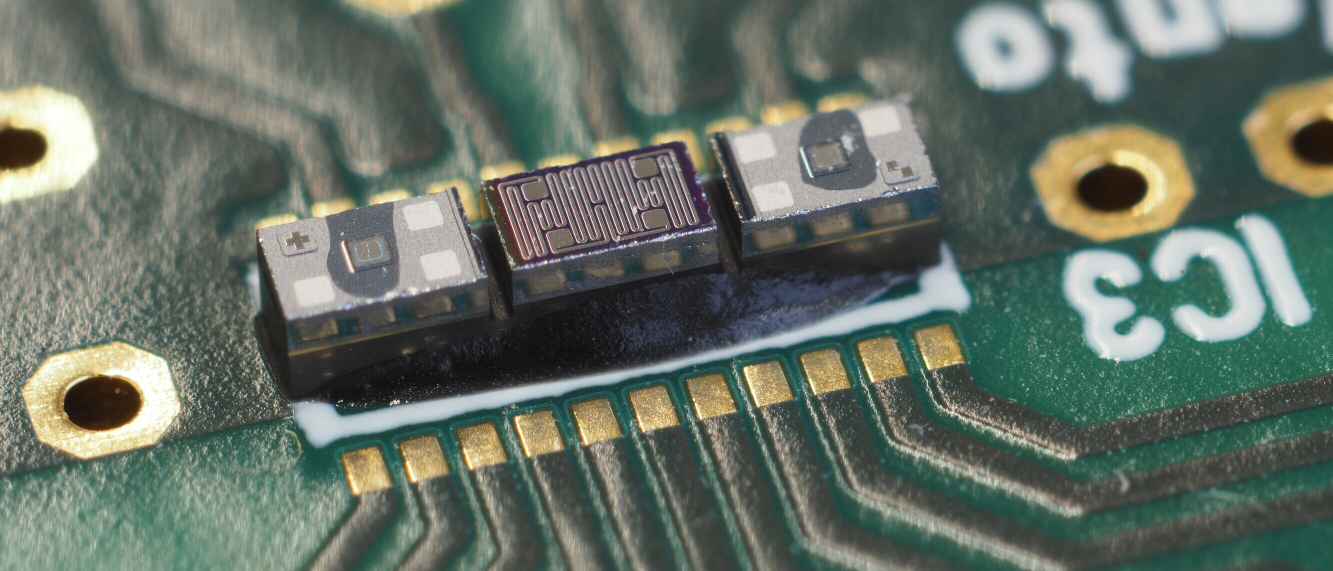
Results: The students successfully completed the fabrication, the assembly and the testing of the air flow sensor device within seven days of practical training. Together with the blended learning sessions, this seminar provided highly valuable insights for motivated students.

Acknowledgements: Performing this course would not have been possible without the support of many individuals and institutions. OST: Roman Willi (IMES) and Mathias Mächler (IMP) devoted their efforts to the sensor concept and testing and to the device fabrication, respectively. IBM Zurich Research Laboratory: Support in annealing the implanted wafers Institut für Ionenstrahlphysik und Materialforschung Helmholtz-Zentrum Dresden - Rossendorf e.V. (HZDR): the efficient implantation service provided by the HZDR at no charge for this Master seminar is kindly appreciated.

Report

Alle News

Report on Masterseminar EVA Semiconductors ‘23

28.11.2023

Fabrication and Test of Semiconductors

The Seminar on Test and Fabrication of Semiconductors is part of the Master of Science in Engineering MSE in Electrical Engineering. The aim is to provide interested students insights into the design, fabrication, and testing of semiconductor devices.

OLYMPUS DIGITAL CAMERA

Results: The students successfully completed the fabrication, the assembly and the testing of the air flow sensor device within seven days of practical training. Together with the blended learning sessions, this seminar provided highly valuable insights for motivated students.

Acknowledgements: Performing this course would not have been possible without the support of many individuals and institutions. OST: Roman Willi (IMES) and Mathias Mächler (IMP) devoted their efforts to the sensor concept and testing and to the device fabrication, respectively. IBM Zurich Research Laboratory: Support in annealing the implanted wafers Institut für Ionenstrahlphysik und Materialforschung Helmholtz-Zentrum Dresden - Rossendorf e.V. (HZDR): the efficient implantation service provided by the HZDR at no charge for this Master seminar is kindly appreciated.

Report